Exploring the Backbone of Modern Electronics: PCB Design
The Critical Role of Printed Circuit Boards in Technology
Discover how printed circuit boards empower electronic advancements and innovation, serving as the fundamental component in every electronic device.
Importance of PCB Design
Why PCB Design is Pivotal in Electronics
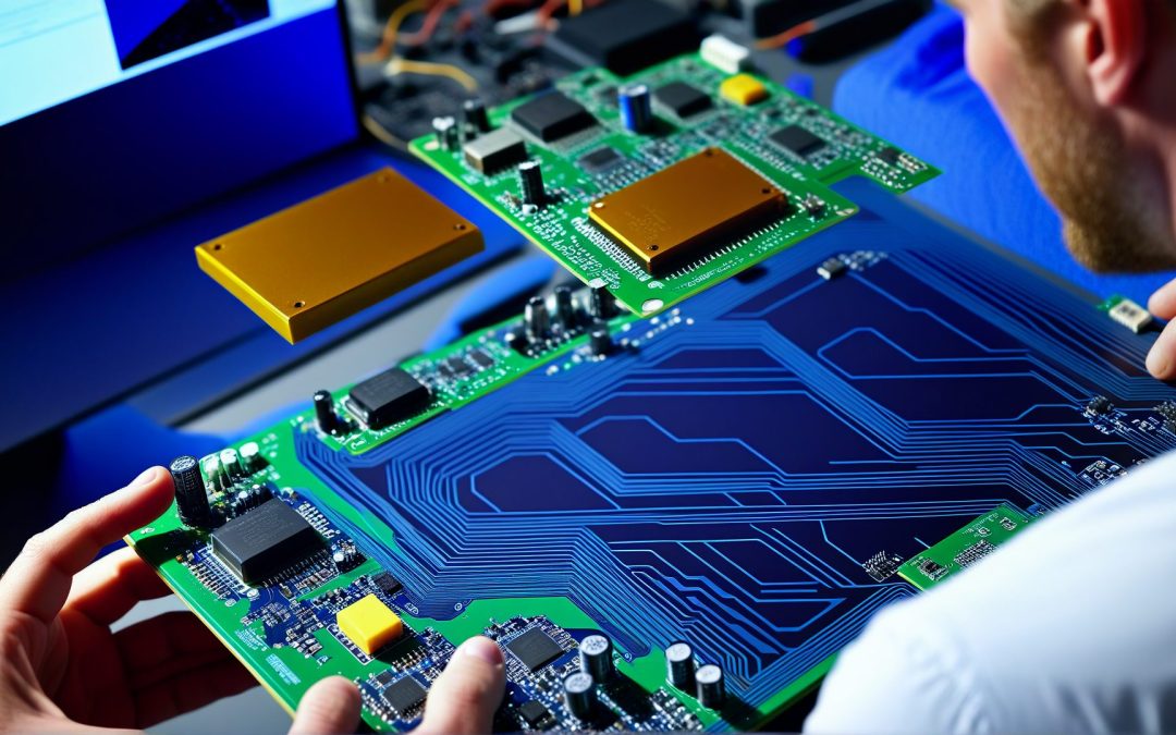
Printed Circuit Board (PCB) design is crucial within the electronics industry as it provides the necessary electrical interconnections and mechanical support for electronic components. This design process ensures that all components fit into a compact, efficient package, vital for the functionality and integration into final products. PCBs not only facilitate complex electrical connections but also maintain the structural integrity required to withstand operational stresses.
Key Features of PCBs

Copper Conductors
Electrical Connections
Mechanical Support
Compact Packaging
Core Structure of PCBs
Understanding PCB Layers and Composition
Printed Circuit Boards (PCBs) are ingeniously crafted with alternating layers of conductive copper and electrically insulating materials. This design ensures optimal electrical connectivity and robust mechanical support for various electronic components. Key conductive features of PCBs include copper traces, pads, and planes, which are essential for the transmission of signals across the electronic device. The mechanical integrity of the board is maintained by the insulating material, which is laminated between the conductive layers, forming a durable and reliable structure.
PCB Fabrication Techniques
Steps in Crafting a Printed Circuit Board
The fabrication of a printed circuit board involves several precise and critical steps. Initially, the board undergoes a plating process to ensure that all conductive areas are adequately covered. Following this, a non-conductive solder mask is applied over the board to protect the copper traces and prevent electrical shorts. The final step in the PCB fabrication process includes the application of a silkscreen layer, which provides a legend for identifying and placing electronic components accurately on the board.
PCB Assembly Process
From Bare Board to Functional PCBA
The assembly of a printed circuit board (PCBA) is a detailed process where electronic components are precisely soldered onto the PCB. This step is crucial as it transforms a bare board into a fully functional electronic assembly capable of performing designated tasks within electronic devices.
Once the components are securely soldered, the PCBA undergoes rigorous testing to ensure all parts function correctly and meet the required specifications. This testing phase is vital to guarantee the reliability and performance of the final electronic product.
Discover the Future of Electronics with Our PCB Design Webinar
Unlock the secrets of efficient PCB design and elevate your electronic projects! Join our free webinar to explore the intricacies of Printed Circuit Board design, learn from industry experts, and see how advanced PCB technology can revolutionize your approach to electronics. Don’t miss out on this opportunity to enhance your skills and knowledge!