Tracing the Evolution of PCB Design
From Bakelite to High-Density Interconnects: The Journey of PCBs
Explore the transformative history of printed circuit boards (PCBs) and discover how advancements in technology have revolutionized electronic design and manufacturing.
Early PCBs
Initially crafted from bakelite, early PCBs featured tangled wires and bulky components, complicating debugging and reliability.
Modern PCBs
Today’s PCBs utilize advanced HDI technology, supporting thousands of tiny, densely-packed connections essential for modern electronics.
The Evolutionary Tale of PCB Design
In the early days of electronics, circuits were manually assembled with discrete components connected by a web of wires, mounted on substrates like bakelite. This method was not only space-consuming but also prone to errors, making the debugging process a daunting task.
Manufacturing was labor-intensive and slow, as each component needed to be individually soldered, leading to high costs and limited production capabilities. The transition to modern PCBs marked a significant leap in electronic design efficiency.

Visualizing Early PCB Technology
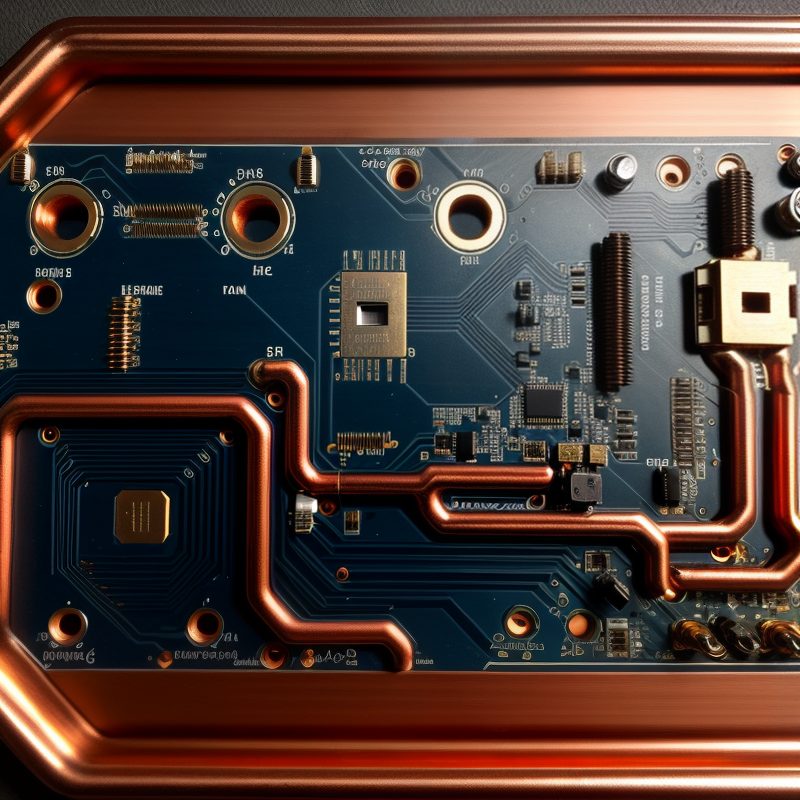
The image below showcases an early PCB design, characterized by exposed copper traces and numerous through-holes, a stark contrast to today’s compact, efficient layouts.
Understanding PCB History
By examining these early designs, we gain insight into the challenges faced by past engineers and appreciate the technological advancements that have shaped modern electronics.

The Evolution of PCB Design
From Manual Assembly to High-Density Interconnects
The journey from the early days of using bakelite substrates and tangled wires to today’s sophisticated high-density interconnect (HDI) PCBs mirrors the incredible advancements in electronic design. Initially, PCBs were cumbersome, with each component manually soldered, leading to high failure rates and difficult maintenance. Modern PCBs, however, utilize advanced manufacturing techniques that embed tiny integrated circuits and passive components directly onto insulating substrates. This shift not only enhances the reliability and functionality of electronic devices but also allows for the miniaturization seen in today’s consumer electronics, medical devices, and aerospace technology.
Modern PCB Complexity
Today’s PCBs feature a remarkable level of complexity.
- Increase in Connection Density 95%
- Growth in Component Miniaturization 85%
- Advancement in Multi-layer PCBs 75%
Discover Cutting-Edge PCB Designs
Step into the future of electronics with our innovative PCB design solutions. Whether you’re looking to upgrade your current systems or are curious about the potential of high-density interconnect technology, our team is here to guide you. Explore our services and see how we can help power your next big idea with state-of-the-art PCB technology.

